History and Types of Microscopes
| ✅ Paper Type: Free Essay | ✅ Subject: Engineering |
| ✅ Wordcount: 3478 words | ✅ Published: 30 Aug 2017 |
What is a microscope?
There is so many little objects that human eyes can’t be able to see. The microscope is a tool to see minute objects consisting of lens or combination of lenses[1]. Due to their highly-improved lenses, we can observe high-quality images and these days this images can be transferred to computers. Today’s microscopes are so advanced that they can show objects which are sized of the millionth part of a meter called micron[2].
The science of searching small objects with microscopes is called microscopy. Microscopic means that impossible to see, without a help of a microscope, with a naked eye[3].
History of Microscope
After the glass is first made in the first century, Roman’s was trying to make objects to be seen bigger. The first and simple forms were called flea glasses and they were able to show 6 times bigger[4].
The microscope is developed in Netherlands at the 1590s but its inventor is not easy to identify. Some proofs are leading to Cornelis Drebbel[5]. But others insist that Zacharias Jansen and his father Hans were working with lenses, they combined some lenses and put them into a tube and invented the microscope. Few others believed that Galileo Galilei was the first discoverer of microscope[6].
First microscopes were not good enough to use at researches because it can only enlarge by 9 times bigger[7].
First, the real microscope was used by Anton van Leeuwenhoek in the late 17th century which was made by pipes, simple lens, plate and screw(Figure1).
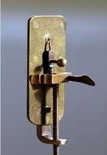
Figure 1
Unlike the others, his microscope could show objects one-millionth of a meter bigger of its sizes(270x). Others best achievement was 50x magnification. With this microscope, he saw and identified bacteria, erythrocyte, and sperm cells. He published their drawings on Philosophical Transactions of the Royal Society of London at 1674.These drawings were forgotten until there were huge developments in science[8].
In 1665 Van Leeuwenhoek’s work was a guide to Robert Hooke and he wrote Micrographia. It is the first book that provides microscopic pictures of insects, plants etc. [9] (Figure 2).
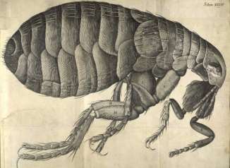
Figure 2-Drawing of an insect by Robert Hooke[10]
After 200 years from Robert Hooke, German engineer called Carl Zeiss improved lenses of the microscope and he established a company named Zeiss. After that, he hired Ernst Abbe to the company. Abbe improved the microscopes and lenses[11].
Types of microscopes
Stereoscope
Dissection microscope is used with visible light. It is used to see dissection better.
It has 3-dimensional images and it has low magnification.
Figure 3 – earthworm captured by Stereoscope
Confocal Microscope
Confocal laser scanning microscopy (CLSM) plays the most significant role on imaging tiny samples in three-dimensional form. CLSM works like an optical microscope with some differences. It uses monochromatic laser light instead of visible light [12].CLSM has widely used from cell biology, genetics, microbiology and development biology to quantum optics, nanocrystal imaging and spectroscopy[13].
History of Confocal Microscope
Early in 1940, Hans Goldmann from Switzerland invented a slit lamp to make documentation of eye examinations. Some researchers believe it might be first confocal optical system [14].
Marvin Minsky invented first confocal scanning microscope in 1955 and in 1957 got its patent.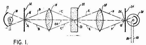
Figure 4: Marvin Minsky’s patent application that shows the principle of CLSM [15].
By moving the stage, illumination point in focal plane could be scanned [16].
In 1969 M. David Egger and Paul Davidovits described the first CLSM in two pages and published. Only one illumination spot generated with this point scanner. It was used for the imaging of the nerve tissue [17, 18].
In 1983 confocal microscope was first used and controlled by a computer after the publication of first work by I. J. Cox and C. Sheppard from Oxford University. Based on Oxford group’s designs, first CLSM was offered from 1982 [19].
At the Laboratory of Molecular Biology in Cambridge, William Bradshaw Amos and John Graham White and colleagues invented the first confocal beam scanning microscope in the middle of 1980s.This time the illumination spot was moving but not the stage. This technique allowed faster image acquisition, four images per second [20].
Working Principle of Confocal Microscope
For getting higher intensities a laser is used. The laser light reflects from the dichroic mirror. After that it hits mirrors on motors and across the sample lasers get scanned by these mirrors. And emitted light passes through the dichroic mirror and gets focused onto pinhole. Finally, the detector measures that light. As it appears the complete image of the sample cannot be observed just one point can be observed. The photomultiplier detector is connected to a computer and one pixel at a time it builds an image [21].
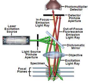
Figure 5: Principal Light Pathways in Confocal Microscopy [22].
What is the advantage of using a confocal microscope?
By scanning lots of thin parts of a sample, it is easy to build a very good three-dimensional image. Confocal microscope has better resolution horizontally and vertically. The best resolution can be obtained at 0.2 microns for horizontal and 0.5 microns for vertical [23].

Examples
There are some examples of imaging with the confocal microscope.
Figure 6: Nematode. Miami University in Oxford, Ohio [24].
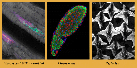
Figure 7 : Example image of confocal microscope [25].
Scanning Electron Microscope (SEM)
SEM is an electron microscope that uses the focused beam of electrons to images of the sample. Electrons interact with atoms in the sample and gives information about external morphology (texture), chemical composition, and crystalline structure and orientation of materials making up the sample [26].A beam of electrons uses raster scan pattern which is a rectangular pattern of an image and reconstruction in the screen. Most computers use bitmap image systems to store the image [27].
The image is created by matching the position with the perceived signal. SEM can get better than 1 nm resolution. Standard SEM microscopes are generally suitable for dry and conductive surfaces in high vacuum. Also, there are specialized machines that work under changeable conditions from low temperature to high temperature and in low vacuum. There is environmental SEM for wet conditions.
McMullan presented the history of SEM [28]. Manfred von Ardenne invented SEM in 1937. In the early 1960s, Cambridge groups marketed as Stereoscan in 1965[28, 29].
After interaction of high energized beam of electrons and outer orbit electrons of sample’s atoms Auger electrons which have low electrons will be formed. These electrons carry information about sample surface.After interactions, there will be electron beams which have lower energy, move to the surface of the sample and will gather there.These electrons called as secondary electrons. For imaging for SEM, mostly secondary electrons are being used. Change of secondary electrons numbers depends on the topography of surface and angle of the point where the beam hits the surface [30].
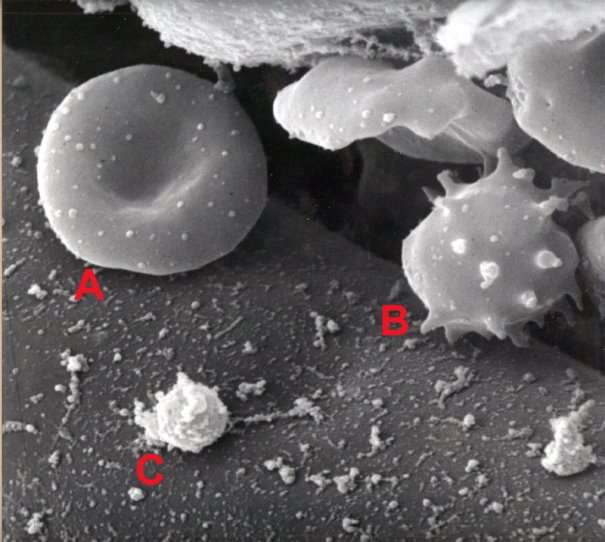
Figure 7: Blood image by SEM [31].
Transmission Electron Microscope
High energized electrons pass through the very thin sample. After interaction of electrons, images are enlarged and focused on fluorescence screen, photographic film layer or CCD camera [32].
In 1930 Max Knoll and Ernst Ruska invented TEM [33]. It allows us to see smaller objects than the optical microscope.
TEM is used in cancer research, virology, materials science, nanotechnology, and semiconductor.
TEM’s contrast depends on absorption of electrons, thickness, and composition of the sample. Complex wave interactions at higher magnifications modulate the intensity of the image with analysis of an expert for the image. The resolution limit is up to 0.2 nm for TEM.
Compared to SEM, TEM has troublesome work to get the sample ready and the user must have a very good background about it [34].
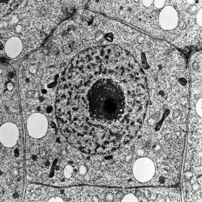
Figure 8: Example of TEM of a plant cell [35].
Compound Light Microscopes
Compound microscopes are 2-dimensional light microscopes and they are most used microscopes. Even though it has low resolution it has high magnification.
Figure 9-meiosis seen by compound microscope[36].
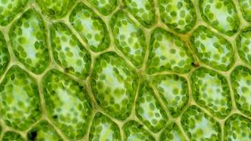
Figure 10-Microscope view of plant cells[37].
Parts of Optical Microscope
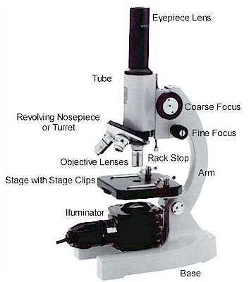
Figure 10 – Parts of a microscope[38]
- Eyepiece Lens: The lens that allows us to see through.
- Tubes: It helps eyepiece to connect to lenses.
- Arm: Holds the tube.
- Base: Supports the microscope at the bottom.
- Illuminator: Light source or a mirror that helps us to see a sample from the tube. If it is a mirror it can reflect outer light to use.
- Stage: This platform is used to put samples and it has clips to prevent the sample from moving.
- Revolving Nosepiece or Turret: This part is for holding lenses together and it can rotate to switch between lenses.
- Objective Lenses: These lenses are most commonly can be put three or four lenses on the microscope. They have 4,10,40 or 100 times bigger magnification. They are color coded and should build to DIN standards.
- Rack Stop: It is used to protect the objective lens from breaking[39].
DIN Standards
The real image is formed 160mm away from the objective lens.
Parfocal distance should be 45 mm.
Eyepiece lens should be 170mm[40].
Working Principle of Optical Microscope
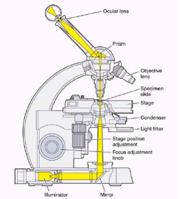
Figure 11 [41]
As shown in Figure 9 light starts its journey from illuminator and with a mirror it reaches to sample. Then it goes to prism through objective lenses. It reflects from the prism and comes to eye in the tube. When light passes through the objective lens makes the image of sample bigger and focuses 160 mm inside the tube and then ocular lenses magnifies the image of sample 25cm away from the eye. This image is a virtual image of the sample (Figure 10). Typical microscopes have four different objective lenses. Scanning (5x), low power(10x), medium power (20x) and high power lenses (40x). We can easily calculate the magnifying of the microscope with multiplying objective lens and ocular lens. For example, after image magnified by objective lenses 40 times of original image of the sample, will magnify second time 20 times bigger by ocular lenses. So, our eye can see 40×20=800 times bigger image of an original image of the sample.
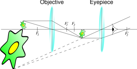
Figure 12 [42]
Differences Between Electron and Light Microscope
- Light microscopes techniques are simple but for electron microscope high-level technical skill needed.
- Preparation time of the sample is few minutes to few hours for light microscopes but several days for electron microscopes.
- Live or dead samples can be seen in light microscopes but for electron microscopes only dead and dried samples can be seen.
- Light microscopes have low resolution than electron microscope and the resolution limit for the light microscope is 200 nm but for SEM 1nm and for TEM 0.2 nm.
- Light rays are used to illuminate for light microscope but for electron microscope electrons are being used.
- Lenses are made of glass for light microscope but for electron microscope all lenses are electromagnets.
- Magnification of light microscope is 500x to 1500x but for EM 160,000x and photographic magnification is 1000,000x or more.
- Light microscopes are cheap but electron microscopes are expensive [43].
Calculation of Resolution
If we want to get good details of very small objects like cells, we need to increase the resolution. It can be described as to see different between two small and very near objects. It can be affected of the wavelength of light and power of lenses. Mathematical formula of separating two different small objects which have the smallest distance (dmin);
Dmin = 1.22 x wavelength / N.A. objective + N.A. condenser
Different then the theoretical power, in practice sample’s quality affects its resolving power[44].
Definition of Numerical Aperture(N.A.) is a value of objectives defined by Abbe.
Numerical Aperture (NA)=n-sin(µ) or n-sin(α)
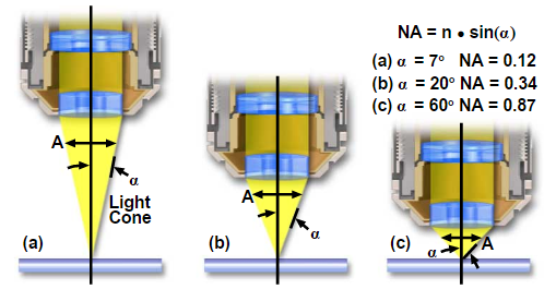
Figure 13 – Numerical Aperture
As shown in Figure 11 light waves go through a sample to the objective lens. But when it comes to practice it is nearly impossible to get the value of aperture above 0.95 with dry objective lenses. When the light cones get the bigger degree of α starts to increase from 7 to 60 and N.A. increases from 0.12 to 0.87. In today’s world, it is possible to use alternative media to make images in water (refractive index = 1.33), glycerin (refractive index = 1.47), and immersion oil (refractive index = 1.51) by the objective lens. We can clearly see Figure 12 and Table 1; highly corrected objectives have bigger N.A.
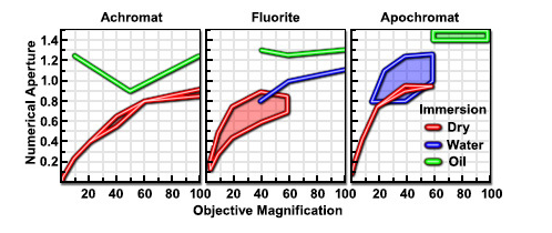
Figure 14
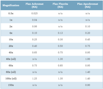
Table 1 – Numerical Aperture versus Optical Correction[45]
There is a limit of resolution in optical microscopes as shown below;
- Let N.A. be 1.4 and resolution is different for lights wavelength.
- A minimum distance of two points of the image is 0.61 λ/N.A.
- As we know visible light wavelength is between 400-700 nm.
- There will be no resolution between two objects if distance is 1/3 λ.
- If we choose green light λ = 500nm and r=0.61 x 500nm / 1.4 =218 nm.
- If we choose blue light λ = 400nm and r=0.61 x 400nm / 1.4 =174 nm.
- If we choose green light λ = 700nm and r=0.61 x 700nm / 1.4 =305 nm[46].
Diffraction Limit of Electron Microscope
Electron microscope has diffraction limit and it is 1nm for SEM, 0.3nm for TEM. This limit occurs because of wave nature of electrons. Electrons has a phenomenon called wave-particle duality. Particle of matter (incident electron) can be explained as wave. We can assimilate to sound or water waves.
Louis de Broglie says that the wavelength of a particle can be calculated as following formula:
λ=h/p
λ: wavelength of a particle
h: Planck’s constant (626×10-34)
p: momentum of a particle
Momentum is the product of mass and the velocity of a particle and equation can be written as;
λ= h / mv
Accelerating voltage determines the velocity of the electrons we can use following formula;
eV = mv2/2
We can calculate the velocity of electrons by;

Due to these formulae, we can show the wavelength of propagating electrons at a given accelerating voltage;

Since the mass of an electron is 9.1 x 10⁻³¹ kg and e = 1.6 x 10⁻¹⁹;
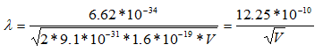
So, the wavelength of electrons is 3.88pm when the microscope is operating at 100 keV, 2.74 pm at 200 keV, and 2.24 pm at 300 keV.
We know electrons in an electron microscope reach %70 of speed of the light wit accelerating voltage of 200 keV, there are effects which are significant length contraction, time dilation, and an increase in mass. By these changes;
c: speed of the light (299 792 458 mps)
So, wavelength of an electron at 100 keV, 200 keV, 300 keV in electron microscopes is 3.70 pm ,2.51 pm, and 1.96 pm, respectively [47].
Another reason for limitation for TEM is, sample transparency has to be proper for electron transparency. To be more precise its thickness has to be 100nm or less.
Electrons can be deflected in magnetic fields by the Lorentz force. This problem may make crystal structure determination virtually impossible [48, 49].
Diffraction Limit of Optical Microscope
There is a limit for imaging with an optical microscope called Abbe diffraction limit. This limit is λ/2(λ is imaging radiation’s free-space wavelength) [50]. Modern works show us that this limit can be passed and can make optical microscopes lenses to have a high resolution[51].
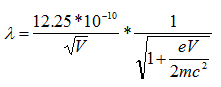
But with diffraction limit even though the lens is corrected there will be blur image of the point. This called Airy disk or diffraction. British mathematician Lord George Biddel Airy has found it. We can see its cross section and appearance below (Figure 13).
Figure 15
Diameter of the disk is;
Bdiff =2.44 λ (f/#)[52]
With f/# limitation can be controlled and wavelength of the light. The maximum resolving power of the lens is determined by this limitation. If we want to calculate diffraction limit we can use following formula;

If we reach the limit lens will become unable to resolve greater frequencies. In theory, if the contrast is %0 the diffraction limit will appear to be as shown in Table 2 at different f/#s for 0.520 μm light as known as green light.
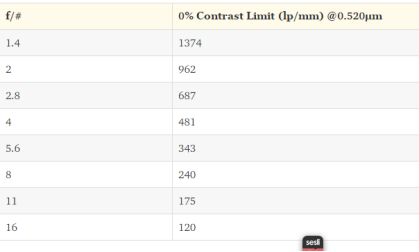
Table 2[53]
Different Ways to Break Resolution Limit of Optical Microscope
There are several ways to break resolution limit of optical microscope. To do that researchers change lenses or different parts of microscopes. Here are some examples:
- By employing stimulated emission to inhibit the fluorescence process in the outer regions of the excitation point-spread function[54].
- By using laterally structured illumination in a wide-field, non-confocal microscope(This method claims that spatially structured excitation light illuminates the sample) [55].
- By improving the lenses with ZrO2.
Synthesis of ZrO2 Nanoparticles
Zirconium(IV) isopropoxide−2-propanol complex (5.6 g) and anhydrous benzyl alcohol (55mL) were charged into a 100 mL Teflon-lined autoclave. This Teflon-lined autoclave was sealed and placed into an oven at 240 °C for 4 days and then cooled to obtain a white turbid suspension. [56].
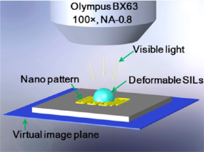
Figure 16[57].
Figure 16 is a schematic of hSIL integrated with an Olympus optical microscope for super-resolution imaging of the underlying nanopattern. The hSIL collects near-field information on the nanopattern and forms a virtual image that can be captured by the objective lens[57].
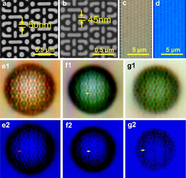
Figure 17 -Super-resolution optical imaging through hSIL on 45 nm gaps. SEM images of the chip with periodic structures of 50 nm gaps (a) and the gold-coated chip with 45 nm gaps (b). (c, d) Optical images of the chip with 50 nm gaps under white and filtered blue light (λmax ≈ 470 nm) without SILs. (e1, e2) Optical images of the chip with hSIL of h/d = 0.8 (d = 11.5 μm). (f1, f2) Optical images of the gold-coated chips through SIL of h/d = 0.78 (d = 10.5 μm) and (g1, g2) with hSIL of higher h/d = 0.84 (d = 11.3 μm). Optical images of e1−g1 and e2−g2 were taken under white light and filtered blue light, respectively. The corresponding image magnification factors of e2, f2, and g2 are 3.1, 2.9, and 3.6. The scale bars for e1−g2 are the same as that of c[58].
References:
1.http://www.life.umd.edu/cbmg/faculty/wolniak/wolniakmicro.html
2.http://www.kurallarinelerdir.com/2016/04/mikroskop-nedir-mikroskobun-tarihi.html
3.https://en.wikipedia.org/wiki/Microscope
4.http://www.history-of-the-microscope.org/history-of-the-microscope-who-invented-the-microscope.php
5.Albert Van Helden, S.D., Rob Van Gent, Huib Zuidervaart, The Origins of the Telescope. 2010.
6.Jay, S., Chapter 2: The Sharp-Eyed Lynx, Outfoxed by Nature. The Lying Stones of Marrakech: Penultimate Reflections in Natural History, 2000.
8.http://www.history-of-the-microscope.org/history-of-the-microscope-who-invented-the-microscope.php
9.https://en.wikipedia.org/wiki/Micrographia
10.http://www.bl.uk/learning/timeline/large107702.html
11.http://www.zeiss.com/corporate/int/history/founders.html
12.Littlejohn, G.R., et al., Perfluorodecalin enhances in vivo confocal microscopy resolution of Arabidopsis thaliana mesophyll. New Phytologist, 2010. 186(4): p. 1018-1025.
13.Hoffman, A., et al., Confocal laser endomicroscopy: technical status and current indications. Endoscopy, 2006. 38(12): p. 1275-1283.
14.Goldmann, H., Spaltlampenphotographie und – photometric. Ophthalmologica, 1939. 98(5-6): p. 257-270.
15.Minsky, M., Microscopy Apparatus. US Patent 1961. 3.013.467.
16.Minsky, M., Memoir on inventing the confocal scanning microscope. Scanning, 1988. 10(4): p. 128-138.
17.Davidovits, P. and M.D. Egger, Scanning Laser Microscope. Nature, 1969. 223(5208): p. 831-831.
18.Davidovits, P. and M.D. Egger, Scanning Laser Microscope for Biological Investigations. Applied Optics, 1971. 10(7): p. 1615-1619.
19.Cox, I.J. and C.J.R. Sheppard, Scanning optical microscope incorporating a digital framestore and microcomputer. Applied Optics, 1983. 22(10): p. 1474-1478.
20.White, J.G., W.B. Amos, and M. Fordham, An evaluation of confocal versus conventional imaging of biological structures by fluorescence light microscopy. The Journal of Cell Biology, 1987. 105(1): p. 41-48.
21.http://www.physics.emory.edu/faculty/weeks//confocal/
22.https://www.microscopyu.com/techniques/confocal/introductory-confocal-concepts
23.Prasad, V., D. Semwogerere, and R.W. Eric, Confocal microscopy of colloids. Journal of Physics: Condensed Matter, 2007. 19(11): p. 113102.
24.http://www.cas.miamioh.edu/mbi-ws/microscopes/confocal.html
25.http://depts.washington.edu/keck/intro.htm
26.http://serc.carleton.edu/research_education/geochemsheets/techniques/SEM.html
27.Leblanc, M., Etude sur la transmission électrique des impressions lumineuses. La Lumière électrique, 1880.
28.McMullan, D. An improved scanning electron microscope for opaque specimens. Proceedings of the IEE – Part II: Power Engineering, 1953. 100, 245-256.
29.von Ardenne, M., Das Elektronen-Rastermikroskop. Zeitschrift für Physik, 1938. 109(9): p. 553-572.
30.Smith, K.C.A. and C.W. Oatley, The scanning electron microscope and its fields of application. British Journal of Applied Physics, 1955. 6(11): p. 391.
31.http://metassoc.com/services/scanning-electron-microscopy/sem-eds-application-examples/
32.Crewe, A.V., J. Wall, and J. Langmore, Visibility of Single Atoms. Science, 1970. 168(3937): p. 1338-1340.
33.http://www.nobelprize.org/nobel_prizes/physics/laureates/1986/perspectives.html
34.Meyer, J.C., et al., Imaging and dynamics of light atoms and molecules on graphene. Nature, 2008. 454(7202): p. 319-322.
35.http://www.vcbio.science.ru.nl/en/image-gallery/electron/
36.http://www.cas.miamioh.edu/mbi-ws/microscopes/types.html
37.http://ichef.bbci.co.uk/images/ic/640xn/p023r74v.jpg
38.http://www.microscope-microscope.org/basic/microscope-parts.htm
39.http://www.microscope-microscope.org/basic/microscope-parts.htm
41.DEVEC°, D.D.E., M°KROSKOP ÇEÅž°TLER° ÇALIÅžMA PRENS°PLER°. Dicle Universitesi.
42.https://www.cs.mcgill.ca/~rwest/wikispeedia/wpcd/wp/o/Optical_microscope.htm
43.http://www.biologyexams4u.com/2012/10/difference-between-light-microscope-and.html
44.http://www.life.umd.edu/cbmg/faculty/wolniak/wolniakmicro.html
45.https://www.microscopyu.com/microscopy-basics/numerical-aperture
46.http://www.math.ubc.ca/~cass/courses/m309-03a/m309-projects/cannon/resolving2.html
47.Bendersky, L.A. and F.W. Gayle, Electron diffraction using transmission electron microscopy. Journal of research of the National Institute of Standards and Technology, 2001. 106(6): p. 997.
48.Thomson, G.P. and A. Reid, Diffraction of cathode rays by a thin film. Nature, 1927. 119: p. 890.
49.Thomas, G. and M.J. Goringe, Transmission electron microscopy of materials. 1979.
50.Abbe, E., Arch. Mikrosk. Anat. 1873.
51.Hecht, L.N.a.B., Principles of Nano-Optics. Cambridge U Press, 2006.
52.Riedl, M.J., Optical Design Fundamentals for Infrared Systems, Second Edition. SPIE Press, Bellingham, WA 2001.
53.http://www.edmundoptics.com/resources/application-notes/imaging/diffraction-limit/
54.Hell, S.W. and J. Wichmann, Breaking the diffraction resolution limit by stimulated emission: stimulated-emission-depletion fluorescence microscopy. Optics Letters, 1994. 19(11): p. 780-782.
55.Gustafsson, M.G.L., Surpassi
Cite This Work
To export a reference to this article please select a referencing stye below:
Related Services
View all


DMCA / Removal Request
If you are the original writer of this essay and no longer wish to have your work published on UKEssays.com then please click the following link to email our support team:
Request essay removal