Micro-Strip Patch Antenna for Wideband Application
| ✅ Paper Type: Free Essay | ✅ Subject: Engineering |
| ✅ Wordcount: 1355 words | ✅ Published: 07 Aug 2017 |
Career Episode 1
CE 1.1 Introduction
This career episode describes about the project which I have done during my vocational industrial training that was undertaken at ‘Krishak Bharati Cooperative Limited’, India in 2009. The title of the project was ‘Design and Fabrication of Micro-Strip Patch Antenna for Wideband Application’. It was completed on time and I was awarded for it. This was my individual project. I was a Diploma student in Electronics & Communication at Sarvoday Polytechnic Institute.
CE 1.2 Background
The project focuses on micro-strip antenna which are small in volumes, have great integration and are cost effective along with providing good performance. I tried to solve its disadvantage of having narrow impedance bandwidth, poor radiation efficiency and low gain. Recently the wideband technology is gaining consideration due to its communication systems that offer reduction in fading, high bandwidth, and low power needs. Wideband receivers make use of narrow band interference suppressions methods that will advance its performance range of communications and capacity. There is problem of jamming of receiver by these narrowband signals on the wideband systems.
The reason for doing this project was its challenge to achieve multi frequency operations and enhancement of the bandwidth of wideband applications. And to solve the issue relating patch antenna having low gain and narrow bandwidth. And majorly to improve its capacity and range of communications.
CE 1.3 Objective of project
There are few methods that have been developed for enhancing bandwidth. They are:
1. by increasing thickness of substrate
2. by stacking different radiating elements of antenna vertically or laterally.
3. low dielectric permittivity
4. utilization of magnetic dielectric substrates.
To form a thick substrate of low dielectric permittivity so that the bandwidth of printed patch increases. There was struggle with this approach for implementation of integrating antenna to other microwave circuits due to its large inductive image of input impedance of antenna and surface wave propagation. Bandwidth greater than 25% is achieved by loading of surface with the help of slots of appropriate shape.
CE 1.4 My obligations
As a team leader, I have many responsibilities and duties which I need to perform with honesty. Few of my duties were:
- To assign tasks to fellow team mates
- Perform research on related topics
- Design the hardware structure and finalize components for use.
- Motivate team members
- Study various reference materials to understand concepts and imply them
- Regularly report project guide about the status of my project
- Troubleshoot the project after its completion
CE 1.5 Personal Engineering Activity
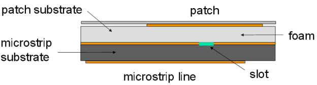
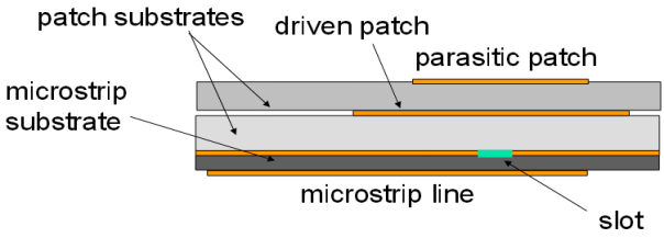
A micro-strip antenna or also known as patch antenna comprises of a dielectric substrate that has a metallic ground plane on one side and a radiating metallic part on the other. They are mostly found in circular, elliptical or rectangle shapes for easy analysis and fabrication purpose. There are few micro-strip antenna that use metal patch mounted above ground plane using dielectric spacers instead of dielectric substrate. Modern printed circuit type technology is used to manufacture micro strip antenna which are relatively cheap. The size of antenna is directly related to wavelength at resonant frequency and employs at ultra-high frequency and high frequency. Below figures show the structures and inner view of micro-strip antennas.

CE 1.6 Design Procedure
I then started with designing of patch antenna. Various steps were involved which are described below. The design of a low-profile patch antenna is very complex. The fact is that the low profile, the wide impedance bandwidth and the omni directional radiation pattern cannot be accomplished simultaneously.
Step 1: Calculate of the patch width
Step 2: Calculate of the effective dielectric constant
Step 3: Calculate of the effective length
Step 4: Calculate of the length extension
Step 5: Calculate of the actual length of the patch
Step 6: Calculate of the ground plane dimensions
The transmission line model is suitable for only infinite ground planes. However, for practical requirements, it is essential to have a finite ground plane. It observed from many literatures that similar results from finite and infinite ground planes can be obtained if the size of the ground plane is greater than the patch dimensions by approximately six times the substrate thickness around the periphery.
CE 1.7
I started with constructing my wideband antenna with double band rejection feature as per my design steps. I did some calculations and then made a study on individual notches and their band notch properties. Proper care was taken to minimize the cross coupling among them and so that the operation is not hampered when integrating the notch elements. Thereafter, two L-shaped slits and an E-shaped slot of varying dimensions are etched on the radiating patch to produce notch characteristics. Then I also implemented a V-shaped strip on ground plane to achieve additional resonances at 15GHz and wide impedance bandwidth at this higher band.
The major parameters affecting the performance properties of micro-strip patch antenna are patch length, width and inset of feed location along with the length and location of slots. By changing the value of ‘⺒, one can determine the required sensitivity for impedance to match and then adjust the electromagnetic coupling between the patch and ground plan along without any extra cost. From my investigation on various design techniques I found the parameter variation of dimension to be the most reliable method.
CE 1.8
I performed come calculation and effective length and dielectric constant can be calculated as “Leff = L + 2ΔL”. Also, the performance of an antenna can be measured considering number of parameters including critical ones like radiation pattern, gain, directivity, bandwidth, return loss and voltage standing wave ratio. Keeping the resonant frequency (fr or fo) as 7GHz and dielectric constant (εr) of 4.4. the height of dielectric substrate (h) is selected as 1.6mm.
I made use of MATLAB application that provide GUI interaction. GUIDE provides tools that are useful in designing user interface for custom applications. It also auto-generates the MATLAB code for construction of GUI and can be modified by user. It can store in two file formats i.e. “. fig” file which as complete code description and “.m” file that has the actual code.
CE 1.9
The major problems I faced while working on this project was in its design. As achieving enhanced bandwidth with multifrequency operations in many of the wideband patch antennas. Also, there was an issue concerning with the low gain and narrow bandwidth due to specifications that are used. And biggest challenge was to achieve good and better-quality performance with increased capacity and having wide range of communication using suppression techniques applied to patch antennas.
CE 1.10
Working within a group during a project is a learning experience. I learnt how to get adjusted with the views and thoughts of other and how to stay connected and focused with each other to fulfill the project commitments and to compete with hassle-free. It taught me new ways to tackle things and situation. Programming and coding were not my forte so I got a chance to understand and gain knowledge about it from my team mates who knew it. At every stage I motivated, interacted and took suggestions from my team mates and gave a fair and unbiased solution and decision, as a team leader to any problem that we faced.
CE 1.11 Summary
I have proposed a small monopole antenna that has the characteristics of single and dual band notches and capability of being used in wideband applications. The antenna in my project works on 2.83GHz to 18.93GHz band and has two rejections between 3.47GHz to 4.33GHz and 5.10GHz to 5.80GHz band range. After performing various measurements and simulation on this project of antenna, it resulted in good relation with voltage standing wave ratio (VSWR) and loss returned. Thus, this thesis had met the objective of designing and simulating the wideband micro-strip patch antenna. It had also provided a sense of attainment as a substantial quantity of work had been accomplished. Nevertheless, there are still significant and vital areas that require further work.
The project held lot of importance in my career as it was my first hands-on experience and that was a part of my curriculum and vocational training. My seniors, guides and professors were appreciating my work and stood by me when needed. This project built my confidence, leadership quality and strengthened my educational skills of electronics.
Cite This Work
To export a reference to this article please select a referencing stye below:
Related Services
View all


DMCA / Removal Request
If you are the original writer of this essay and no longer wish to have your work published on UKEssays.com then please click the following link to email our support team:
Request essay removal