Power-Management based on Reconfigurable Last-level Cache on Non-volatile Memories in Chip-Multi processors
| ✅ Paper Type: Free Essay | ✅ Subject: Engineering |
| ✅ Wordcount: 2775 words | ✅ Published: 23 Sep 2019 |
Power-Management based on Reconfigurable Last-level Cache on Non-volatile Memories in Chip-Multi processors
Abstract— with technology scaling and increasing parallelism levels of new embedded applications, the number of cores in chip-multiprocessors (CMP) has been increased. In this context, power consumption becomes a primary concern in future CMPs because many of them are generally limited by battery lifetime. For future CMPs architecting, 3D stacking of last level caches (LLCs) has been recently introduced as a new methodology to combat the performance challenges of 2D integration. However, the 3D design of LLCs incurs more leakage power consumption compared to conventional cache architectures in 2Ds due to dense integration. In this paper, we propose a power-efficient reconfigurable hybrid last level cache architecture for future CMPs. The proposed hybrid architecture SRAM memory is incorporated with STT-RAM technology for using the advantages of both new and traditional technologies. The Experimental results show that the proposed method minimizes power consumption under multi-programmed and multithreaded applications.
Keywords— Reconfigurable Hybrid Cache, Last Level Cache Non-Volatile Memory, Chip-Multi Processor, Power consumption.
I. Introduction
In recent years, to address the requirement of new data-centric applications for larger memories and to break the memory wall problem, on the other hand, architects have dramatically increased the size of Last Level Cache (LLC) in the memory hierarchy. However, the increasing power consumption not only leads to increased cost and dark area but also leads to an increase of chip temperature. Increasing chip temperature and creating hot spots leads to reliability problems in the chip and reducing chip lifetime. In this regard, some architectures and techniques have been proposed for power management to reduce the dark area in multi/many core systems[1].
Memory modules and cache banks are important components of on-chip storage and have a big portion in total chip-multiprocessor (CMP) and power consumption [2]. Emerging Non-volatile memory (NVMs) technologies with desirable characteristics such as near-zero leakage power, high density and etc. in comparison to the traditional technologies are ideal for using in next-generation CMPs to combat dark silicon. Nevertheless, they suffer from shortcomings such as a limited number of writing operations and long write operation latency and high energy. In order to overcome the mentioned disadvantages, we need to exploit SRAM and STT-RAM as two different types of cache banks. This heterogeneous point of view leads us to the best design possibility with using the benefits of both memory technologies. The major contributions of this paper can be summarized as below:
- Using a proposed hybrid cache architecture that is reconfigured dynamically in runtime to reduce the power consumption by restoring and duplication.
- Analyzing the cache behavior to specify the power-off opportunities based on spatial locality. That is created by different metrics to banks in a Dynamic Non-Uniform Cache Architecture (DNUCA).
- Evaluating power consumption and performance of our proposed design under multi-threaded workloads.
The rest of this paper is organized as follows. Section 2 reviews the prior related works. Section 3 describes the details of the proposed hybrid reconfigurable cache hierarchy with a problem formulation. In Sections 4, experimental evaluation is presented. Finally, section 5 concludes the paper.
II. RELATED WORK
A number of works have been done to reduce power consumption of hybrid memory architectures in embedded systems. In work [3] proposed a hybrid cache with access-aware policies and partition-level wear-leveling scheme to reduce power consumption. The study in [4] focused on a hybrid cache hierarchy, which uses a reconfiguration approach, and a statistical prediction engine to improve system performance in CMP. Their technique is based on this fact that every technology has higher bandwidth in the specific range of capacity so they have used several technologies based on bandwidth demands of running applications. Based on non-uniform cache architecture, many previous works used hybridization of SRAM and Non-Volatile Memory (NVM) technologies that have higher storage density and near zero leakage power consumption to reduce leakage power and energy in LLCs. In research [5] proposed a hybrid SRAM/STT-RAM L2 cache that assigns a write counter to each block of the cache. After writing access to each block of the cache, the related block counter counts up. If the value of the counter passes a predefined threshold, the related block is determined to write intensively and migrated from STT-RAM part to the SRAM part. All of these approaches either use a lot of specific thresholds to distinguish parts of the cache or require high hardware overhead to predict cache behavior. In this paper, we use statistical information instead of using a specific threshold to distinguish banks in a non-uniform cache architecture.

III. Proposed method
Fig. 1 shows a 3D CMP with two processing layers connected by TSVs. The bottom layer is a 4×4 tile-based system that forms a 2D mesh, each tile consists of a core, a private L1 cache, and an SRAM bank of a shared L2 cache. In the top layer, 16 STT-RAM banks are placed as backup L2 cache that they are power-off at the first of workload running.
In this design, we have three aspects: First, a hybrid cache is used (i.e. a large capacity of STT-RAM, together with small-capacity SRAM). Second, STT-RAM banks are divided into two groups that are shared by all cores. As shown in Fig. 1, the banks in orange color are local space in STT-RAM banks that we use them for migration and the banks in gray color are used only for replication. Third, we adopt a DNUCA architecture for the shared L2 banks.

A. Metrics of Interest
Our proposed method consists of two policies: turn-on policy and turn-off policy. There are three factors are used to make decisions.
- Workload intensity (sensitivity): various workloads during their execution are used differently through the entire cache. So, banks due to workloads are divided into read-intensive or write-intensive states. This parameter is defined as the number of writes related to the number of reads in LLC. We use two counters to count the number of LLC writes and the number of LLC reads.
- Manipulation (utilization):this parameter is defined as the number of cache lines referenced in a bank related to total lines in that bank in each period. So, when manipulation for a bank is high, that bank needs much space and has potential power-off opportunities. We use a 32-bits counter for each bank to identify manipulation parameter at each bank. These counters are reset at the beginning of each period. This counter of each bank is increased by one when a line cache is inserted into the corresponding bank and it is decreased by one when the cache line is invalided or evicted.
-
Accessibility (hotness): it is the number of hits to a bank related to the total number of misses in LLC in each period. So, this parameter indicates that if the cache miss rate increase, the bank is power-off. We use three 32-bits counters; a counter to count hit numbers to each clean cache line, a counter to count hit numbers to each dirty cache line, and a counter to count the number of LLC misses for all the cache banks.
Table I. SRAM Power-off Policy.
.
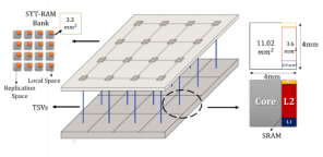
Fig. 1. Overview of the proposed 3D CMP.
B. Power-off Policy
At the first period of workload running, cores are used shared L2 caches in the bottom layer (SRAM) as LLC. At the end of each period, we determine the behavior of each cache bank in the next period by monitoring the behavior of the cache consist of utilization, hotness and sensitivity in that bank. Actually, this information is utilized to guide the power-on, power-off, data replication policy and data migration policy in each bank.
Table I show the overall views of the SRAM power-off policy. When a SRAM bank is read-intensive state and also has the low hotness and the low utilization, the SRAM bank will be powered off because this bank would have few caches misses. But when a read-intensive SRAM bank has the high hotness and the low utilization or the low hotness and the high utilization, first the valid cache lines in the SRAM bank will be migrated to local space in the corresponding STT-RAM bank and next the SRAM bank will be powered off. In read-intensive banks, as the read counts are larger than the write counts, write delay and write energy of STT-RAM has a negligible effect in performance and we can save leakage power by power-off the SRAM bank. In the end, if a read-intensive SRAM bank has the high hotness and the high utilization, the corresponding STT-RAM bank is powered on while the SRAM bank stays power-on and we use both of them. In this state, valid lines also will be replicated to a replication space in an STT-RAM bank to exploit reference locality.
On the other hand, when an SRAM bank is write-intensive and has the low hotness and the low utilization, the SRAM bank will be powered off, similarly. But when a write-intensive SRAM bank has the high hotness and the low utilization, first the valid cache lines in SRAM bank will be migrated to local space in the corresponding STT-RAM bank and next the SRAM bank will be powered off and we use the STT-RAM bank as LLC. In another case, when a write-intensive SRAM bank has the low hotness and the high utilization, the SRAM bank will be maintained turn-on and don’t have any change in that bank, as the majority of accesses are writing, and STT-RAMs suffer write delay and write energy. In the end, if a write-intensive SRAM bank has the high hotness and the high utilization, the corresponding STT-RAM banks are powered- on while the SRAM bank stays turn-on. In this state similar to the read-intensive bank, valid lines also will be replicated to a replication space in an STT-RAM bank to exploit reference locality.
|
Read–intensive bank |
Write– intensive bank |
|||
|
Low hotness |
High hotness |
Low hotness |
High hotness |
|
|
Low utilization |
Turn off SRAM bank |
Migrate the bank from SRAM to corresponding STT-RAM, turn-off the SRAM |
Turn off SRAM bank |
Migrate the bank from SRAM to corresponding STT-RAM, turn-off the SRAM |
|
High utilization |
Migrate the bank from SRAM to corresponding STT-RAM, turn-off the SRAM |
Replicate the bank to central STT-RAMs |
Maintain SRAM bank in turn-on mode |
Replicate the bank to central SRAMs |
Table II shows the overall view of the STT-RAM power-off policy. Due to this table, when a STT-RAM bank is read-intensive and has the low hotness and the low utilization, the STT-RAM bank will be powered off because these parameters show that the importance of the need for LLC is low and thus power-off this bank can remove search delay in this bank. But when a read-intensive STT-RAM bank has the high hotness and the low utilization or the low hotness and the high utilization, the STT-RAM bank will be maintained turn-on. Otherwise, if a read-intensive STT-RAM bank has the high hotness and the high utilization, valid lines in local space in a STT-RAM bank will be replicated to a replication space.
Table III. main Configuration parameters as used in the experiments.
.
.
When a STT-RAM bank is write-intensive and has the low hotness, and utilization respectively, SRAM bank will be powered off, similarly. But when a write-intensive STT-RAM bank has the high hotness and the low utilization, the STT-RAM bank will be maintained turn-on. In case of a write-intensive STT-RAM bank has the low hotness and the high utilization, valid lines will be migrated from local space in a STT-RAM bank to the corresponding SRAM bank and then the STT-RAM bank will be powered off.
Table II. STT-RAM Power-off Policy.
.
.
|
Read-intensive bank |
Write intensive bank |
|||
|
Low hotness |
High hotness |
Low hotness |
High hotness |
|
|
Low utilization |
Turn off STT-RAM bank |
Maintain STT-RAM bank in turn-on mode |
Turn off STT-RAM bank |
Maintain STT-RAM bank in turn-on mode |
|
High utilization |
Maintain STT-RAM bank in turn-on mode |
Replicate to replication space in STT-RAM banks |
Migrate the bank from STT-RAM to the corresponding SRAM, turn off the STT-RAM |
Replicate to replication space in STT-RAM banks |
C. Replication
Replication of data blocks is one of the power-saving approaches in this paper. In other words, the data block location is not limited to a single bank. We use these replicated blocks that waste the capacity of cache due to storing the redundant information to reduce the frequency of costly memory access. Since STT-RAM banks in this paper have overall capacity 4 times SRAM banks, we have the extra capacity to apply replication. But STT-RAM banks suffer from the shortcoming of the limited number of writing operations, therefore we control the amount of replication by using counters for each bank. We distribute the number of writes among free spaces in replication space each bank. We divide the local space each bank into three groups that have the same capacity and use one counter for each group, therefore we totally use 48 counters to distribute writes in STT-RAM banks.
IV. Experimental Evaluation
A. Platform Setup
To evaluate the proposed method, GEM5 simulator with NoC simulator [6] is used to design and simulate our proposed architectures as shown in Fig. 1. The main parameters of the simulation configuration are listed in Table III. Each core has a private L1 instruction and data cache. All cores share a L2 cache that is divided into 64 banks. The area of a core tile in the core layer is 3.5 mm2 estimated by McPAT [7] and CACTI 6.08]. We use synchronization based multithreaded workloads selected from PARSEC [9], SPLASH-2 [10] and Phoenix [11] for multi-thread workloads.
|
Component |
Description |
|
|
Number of Cores |
16, 4×4 mesh |
|
|
Core Configuration |
Alpha 21264, 3GHz, 32nm, 11.01mm2 |
|
|
Private L1 Cache per Core |
SRAM, 4 ways, 64B line size, 32KB per core. |
|
|
Last-level Cache |
Proposed |
SRAM: 2MB L2 (16 bank SRAM, each has 128kB). STT-RAM: 32 MB L2 (64 bank STT-RAM, each has 512kB). |
|
Baseline1 |
L2: 2MB SRAM (16 bank SRAM, each has 128MB). |
|
|
Baseline2 |
L2: 2MB SRAM(16 bank SRAM, each has 128MB). L3 : 8MB SRAM (16 bank SRAM, each has 512kB). |
|
|
Baseline3 |
L2: 2MB SRAM(16 bank SRAM, each has 128MB). L3: 32MB STT-RAM (64 bank STT-RAM, each has 512kB). |
|
|
Network Router |
2-stage worm hole-switched, virtual channel flow control, 2VCs per port, 5flits buffer depth, 8 flits per a data packet, 1 flit per address packet, 16-byte in each flit. |
|
B. Experimental Results
In fig.2, shows the results of the proposed system with other styles. The power consumption is reduced on average by 96.4% compared to baseline-2 and 25.4% compared to basline1.Also is reduced by 10.5% compared to basline3.
Fig. 3 shows the normalized IPC metric. As shown in this figure, the proposed design improves IPC performance on average up to 5.9%, and 33.4% compared with the SRAM-baseline, and fixed-hybrid design, respectively. But, the IPC for proposed hybrid style is reduced by 2.1% on average compared with the baseline1.
Fig. 4 shows the percentage of SRAM and STT-RAM used in the proposed hybrid memory architecture. Our design uses 52% of SRAM and 48% of STT-RAM memories on average for benchmark applications. As illustrated in this figure, for applications which are heavily memory accessed like canneal or read-intensive like streamcluster, the percentage of STT-RAM is more than SRAM. It is because of that the proposed technique turns on STT-RAM banks incorporated with SRAM banks to solve the shortage problem of last level cache for these types of applications. When a workload is read intensive, due to the lower read energy and read latency in STT-RAM in compared to SRAM technology, STT-RAM banks are turned on and corresponding SRAM banks are turned off, therefore, in this scenario, the number of turning on STT-RAM banks are more than turning on SRAM banks. The difference between the percentages of memory technologies in our proposed design can be explained due to the small amount of writing-intensive data blocks or lower leakage energy of STT-RAM in comparison with SRAM.
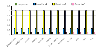
Fig.4: results of power consumption normalized to Baseline 2.
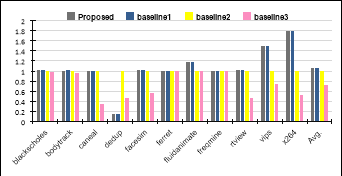
Fig.5: Normalized IPC for various configurations normalized to Baseline 2.
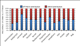
Fig.5: Percentage of SRAM vs STT-RAM contribution.
V. Conclusion
In this work, we proposed a novel reconfigurable last-level cache architecture. In this paper, we propose an energy-efficient reconfigurable hybrid last level cache architecture for future CMPs. In this proposed hybrid architecture SRAM memory is incorporated with STT-RAM technology for using the advantages of both new and traditional technologies. Our results show that our proposed method are effective in improving the average of power consumption (96.4% ) and the performance (5.9%) compared to the state SRAM cache banks.
References
[1] Symposim Comp. Arch (ICAS),pp. 365-376. 2011.
Cite This Work
To export a reference to this article please select a referencing stye below:
Related Services
View all


DMCA / Removal Request
If you are the original writer of this essay and no longer wish to have your work published on UKEssays.com then please click the following link to email our support team:
Request essay removal