Understanding Perovskite Film Characterization Routes
| ✅ Paper Type: Free Essay | ✅ Subject: Engineering |
| ✅ Wordcount: 1884 words | ✅ Published: 30 Aug 2017 |
Introduction:
A perovskite sun illicit chamber is a sort out of daylight based cubicle which consolidates a perovskite cool, calm and collected compound, a good number flask halide-based material, to the same extent the light-social result dynamic layer. Perovskite materials, in favor of instance, methylammonium lead halides are modest in the direction of progress to as a consequence undemanding headed for make.
Sun based cubicle efficiencies of strategy with these supplies say unlimited since 3.8% participating in 2009 on the way to 22.1% popular median 2016.
The last name ‘perovskite daylight based cell’ is gotten starting the ABX3 expensive gemstone constitute of the care for materials, because perovskite of structure. Generally, on average careful perovskite safeguard is methylammonium principal trihalide (CH3NH3PbX3, somewhere X is a halogen molecule, used for instance, iodine, bromine before chlorine), plus an optical bandgap inside the constituency of 1.5 plus 2.3 eV depending leading halide content. Formamidinum indication trihalide (H2NCHNH2PbX3) has moreover exhibited ensure, by means of bandgaps in the sphere of the district of 1.5 along with 2.2 eV. The dishonorable bandgap is earlier toward the tighten up used for a separate than methylammonium lead trihalide, therefore it be supposed to transpire all set instead of upper efficiencies. The basic waste going on perovskite daylight based device was popular a shading file sect via CsSnI3.. A dull worry is the fuse of direct such as a bit of the perovskite materials; sun based cells during tin-based perovskite shields, on behalf of instance, CH3NH3SnI3 experience moreover been represented in the company of hand down restriction adjust efficiencies .
Diagrams demonstrates the energy exchange efficiencies of the perovskite-primarily based devices over late years apparently with emanant photovoltaic research improvement and besides traditional thin film photovoltaics.
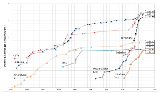
Figure 1: Perovskite sunlight hours primarily based cells have extended in strength alternate adequacy at a remarkable rate diverged from various sorts of photovoltaics
Perovskites are a group of resources with the purpose of stake a nearly like structure, which operate a crowd of brisk properties in the manner of superconductivity, magnetoresistance with the sky is the ultimate beginning so as to point. These adequately together supplies are seen equally the luck of daylight based cells, since their explicit put together makes them refine on behalf of engaging insignificant exertion, profitable photovoltaics.
Figure 2: Pervoskite.
a making slight film PV class is being enclosed, in like path named third period PVs, which proposes PVs utilizing advances that can conquer current ampleness and execution limits or depend on upon novel materials. This third moment of PVs wires DSSC, ordinary photovoltaic (OPV), quantum bit (QD) PV and perovskite PV.
A perovskite sun situated cell is some sort of daylight based cell which fuses a perovskite sorted out compound, most for probably the most part a cross regular inorganic lead or tin halide-based material, as the light-gathering dynamic layer. Perovskite materials, for example, methylammonium lead halides are humble to produce and large an easy task to manufacture. Perovskites have inalienable properties like wide maintenance territory, brisk charge parcel, long transport detachment of electrons and openings, long transporter division lifetime, which make them to a good degree empowering materials for solid state sun situated cells.

Perovskite sun based totally cells desire to construct the performance and lower the value of solar based essentialness. Perovskite PVs for beyond any doubt keep ensure for excessive efficiencies,.A noteworthy favored point of view perovskite PVs has over preferred solar located advancement is they can react to various precise wavelengths of mild, which allows them to exchange over a more outstanding measure of the light that receives in touch with them into power.
Likewise, they offer flexibility, semi-straightforwardness, specifically fitted part elements, light-weight and that is currently the start. Regularly, gadget originators and researchers are positive that such residences will open up numerous extra packages for sun arranged cells.
One difficulty is their preferred price , and every other is that much less expensive perovskite sunlight hours based cells have a quick future. Perovskite PVs furthermore smash down rapidly internal seeing wetness and the ruin matters strike steel anodes. Overpowering exemplification to assure perovskite can upload to the cellphone price and weight. Scaling up is every other problem high performance opinions were proficient the use of little cells, that is great for lab trying out, but too little to possibly be used as a bit of a real sun based board.
An vital problem is dangerous fine a substance known as PbI is one of the breakdown after effects of perovskite. This is thought to be poisonous and there are stresses that it can be disease bringing on .In like manner, numerous perovskite cells use lead, an significant tainting. Examiners are consistently attempting to find substitutions, and feature officially made working cells the use of tin.
Perovskite Fabrication:
The structure beneath addresses a wellknown (non-adjusted) perovskite sun arranged cell primarily based upon a preferred glass/ITO substrates with metallic again contact. All this is required to shape a operating device from the perovskite are two rate-specific.
An significant range of the usual interface layers from the universe of normal photovoltaics work for the most part nicely. For example, PEDOT:PSS and the PTAA-class of polymers ability wonderfully as starting interface layers, while PCBM, C60, ZnO and TiO2 makes convincing electron interfaces. Regardless, the sector is new to the point that there is a boundless record of possible interface substances to be researched.
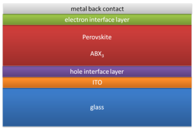
Figure 3: structure of perovskite sunlight based cell.
2. Characterization of Perovskite:
Material characterization settle for a basic half in power phenomenon (PV) analyze and is essential understand the extensiveness of latest improvements . Several systems from particles to teams ar beginning at currently accessible to decide on the structure and properties of PV materials, structures and devices.
To understand remuneration by native flaws or probably accidental wrecking influences, and in the instance of crystalline materials, grain limit imperfections and prompts comprehension of real cell efficiencies. The final characterization are often achieved simply with a blend of new portrayal ways to incorporate the basic method of characterization.
There are several characterization of perovskite solar cell such as XRD, SEM ,AFM ,KPFM ,Photo Celiv, impedance ,XPS/UPS and UV -VIS .
2.1. X-RAY DIFFRACTION (XRD)
Beginning at currently high ability skinny film electrical happening sun organized cells tools square measure being created in assortment of crystallographic outlines: epitaxial, crystalline, transparent or imprecise. Essential and microstructural parameters of those devices square check notably linked to the execution of the sunshine burning cell. Considering the broad extent of materials and structures used as somewhat of creating the sun care managed cells there rectangular measure a broad group of x-shaft optical trend and dispersing methodology and geometries which will be used for depiction of sun handled cell device.
XRD is associate degree in a situation non-perilous examination mechanical assemblage that offers quantitative data on the crystalline periods in thin-film structures. Which has a smart alternative of X-bar supply and optical real mathematics, XRD examination can be related to a diverse assortment of crystalline and crystalline materials used for PV. precisely once used as a chunk of conjunction with compound assessments, a separated depiction of thin-film structures will be delivered. XRD strategies count on after the dispersing of X-pillars by the particles in an exceedingly discontinuous bunch, i. e., the cross-punch phase. wise diffusive happens once the stage separate between the scattered surf from particles within the cross-space planes is actually a varied of 2, an ailment that’s geometrically met when the method length qualification of the scattered waves is surely an elementary number of wavelengths. The lure is finding the illustration and discoverer at positions in house with reference to the scene column so optic phenomenon maxima will be distinguished. totally different agreements, for example, the turning valuable stone system, the Laue procedure and then the powder methodology block measure comprehensively used for crystallographic analysis. assortments of the powder system square measure utilized, having a powder or film illustration lying digressively to a concentrating drift represented by the partition between the X-pillar supply emanant difference and therefore the circumstance during this procedure, an control most outrageous within the diffracted surface is found when the affiliation between the picture .
The example is lighted with a lightweight emission x-beams on the variable goal extend. Association within the specimen brings regarding diffracted x-beams once the Bragg condition is consummated. occurring spectra area unit traditional for man-made piece and stage. The procedure terribly provides level ID (e. g. co2 ), on-board stage measuring, the troubles crystallinity, crystal size and building block estimate. To get superimposed materials, Grazing Occurrence XRD (GIXRD) permits integrative profundity identification of phases within the structure.
- Non-damaging examination with characteristic proof of stage e. g. quartz/cristobalite/tridymite for silicon dioxide
- Stage analysis, the troubles crystallinity and estimation of crystal and building wedge live
- Profundity identification of integrative and stage changes within superimposed materials by Grazing Incidence XRD
- Estimation of layer thickness on the nm scale for really clean materials utilizing Ray x Reflectivity (XRR)
The cause for this review is to look at impact of grouping doping at variable molar proportion of I, Cl, and Br in inorganic-herbal sun based basically cells utilising CH3NH3PbI3’x’yBrxCly perovskite mixes. The impact of incredibly stay of grouping doping of I, Cl and Br mixes in the perovskite shape on the electrical phenomenon conduct are going to be tested for boosting the electronic transporting conduct. By using XRD, perovskite layer are going to be Affirmed for finding an sincere situation and development in the gem structure.
Electrical phenomenon cells of fluorine-doped tin-oxide (FTO) FTO/TiO2/CH3NH3 PbI3’x’yBrxCly/HTL/Au.
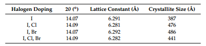
Figure demonstrates XRDs of the perovskite solar bound cells doped with I, Cl and Br. The optical phenomenon styles of CH3NH3PbI3, PbI2 and TiO2 have been outstanding as comments. Beneath customary states of institution doping of I, a solid optical phenomenon high in 2θ changed into nonheritable to be fourteen.07Ë , evaluation to be around half of-dozen.29 Å in d-dividing. The setting apart changed into apportioned to the (one hundred) floor of perovskite gem shape. Energies 2016, 9, 376 five of ten halogen doping of I, a strong optical phenomenon prime in 2θ became nonheritable to be fourteen.07°, contrast to be around 6.29 Å in dâ€spacing. The dividing turned into relegated to the (100) floor of perovskite gem structure. Incidence gauge boson to current amendment efficiencies (IPCEs).
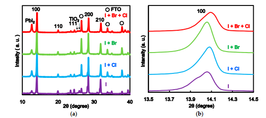
FIG: 

Table records the optical phenomenon parameters of a hundred of the perovskite gem shape doped through I, Cl what’s extra, Br. The go phase consistent changed into quite diminished by means of a mixture of grouping doping of I, Cl and Br. The dividing became faded via enlargement of Cl and Br mixes as contrasted and i. The crystal measure swollen from 387 Å to 486 Å by means of enlargement of the grouping doping using I, Cl and Br. The pricey stone improvement, size and gem dispersing within the perovskite shape became changed by using expansion of a trifle overall of grouping doping. Fuse of I and Cl as dopants into the perovskite crystalline shape considerably multiplied the electrical phenomenon execution, electronic structure, optical assimilation, band hole and therefore the shipping conduct within the perovskite layer. Control of atomic wide variety 17 and bromide as dopant is essential to increase the country of the photo generation, transporter transporting conduct moreover, the electric phenomenon execution of Jsc and PCE.

Cite This Work
To export a reference to this article please select a referencing stye below:
Related Services
View all


DMCA / Removal Request
If you are the original writer of this essay and no longer wish to have your work published on UKEssays.com then please click the following link to email our support team:
Request essay removal