Surface State in Bi1.5Sb0.5Te1.7Se1.3 Nanoflakes
| ✅ Paper Type: Free Essay | ✅ Subject: Physics |
| ✅ Wordcount: 2442 words | ✅ Published: 01 Feb 2018 |
Result of a study on the surface state in Bi1.5Sb0.5Te1.7Se1.3 nanoflakes
4.1 Introduction
The recent discovery of topological insulators (TIs) has provided new route for producing low-dimensional relativistic electronic states. The exotic surface states of TIs have attracted the attention of scientists because of their fascinating physical properties and applicability in spintronics and quantum computations [24-28]. The unique surface states were confirmed by angle-resolved photoemission spectroscopy (ARPES) experiments and scanning tunneling microscopy (STM) on Sb2Te3, Bi2Te3, and Bi2Se3 [29-34]. Magnetotransport studies have also provided a clear picture of the topological surface state and the ° Berry phase shift [35, 36],which gives rise to the immunity of Dirac fermions to localization. Bi2Te3 and Bi2Se3 are suitable candidates for TI studies because of their large energy gaps. Eg is approximately equal to 0.3 eV and 0.17 eV. However, the metallic bulk conduction of natural imperfections, such as vacancies or antisite defects in these materials, makes it difficult to probe surface Dirac fermions. Therefore, a high-insulating bulk state is a prerequisite for transport property studies of TIs. Substantial effort has made it possible to examine both the surface and the bulk channels either through electrical gating [36-42] or substitution doping [12-14, 42]. Recently, it was discovered that Bi2-xSbxTe3-ySey (BSTS) is a high-insulating bulk TI. BSTS exhibits a tetradymite structure, a low carrier concentration (2.3 × 1016 cm–3), and a large bulk resistivity (8 Ω cm) because of the ordered occupation of Te/Se in the quintuple-layer unit [12, 13]. However, a reliable detection of surface quantum oscillations is difficult in BSTS flakes because of the inhomogeneous defect [12] and low surface mobility [40]. Thus, the low mobility in a bulk channel plays a crucial role in probing surface quantum oscillations.
In this chapter, we report the observation of surface-dominated transport in the topological insulator BSTS nanoflakes. Shubnikov-de Hass (SdH) oscillations study on the 200-nm BSTS nanoflake indicates that the achievement of surface-dominated transport can be attributed its high surface mobility of 2602 cm2/Vs (top surface), 3657 cm2/Vs (bottom surface), and low bulk mobility of 12 cm2/V s, which is a much lower value than those reported [12-13, 40-41]. Besides, the nontrivial Dirac surface state was further confirmed by the weak anti-localization (WAL) effect and the semiconducting to metallic transport transformation as the thickness of the specimen was reduced to the thin film limit, in which a up to 90% contribution from the surface channel was estimated based on the thickness dependence of the electrical conductance and the result of the SdH oscillations.
BSTS single crystals nominally composed of Bi1.5Sb0.5Te1.7Se1.3 were grown by melting the mixture of Bi (99.999%), Sb (99.999%), Te (99.999%), and Se (99.999%) in sealed evacuated quartz tubes. First the mixture was slowly ramped up to 750 °C at a rate of 100 °C/h and kept at 750 °C for 12 h. It was then furnace cooled to room temperature at a rate of 100 °C/h. The sample was reground and sintered again. The same procedure was repeated three times to ensure sample homogeneity. Finally, the sample was heated to 800 °C for 48 h, then cooled to 500 °C and annealed for 96 h.
The crystal structures of the samples were identified using powder X-ray diffraction and refined using the General Structure Analysis System (GSAS) software package equipped with the EXPGUI interface, as shown in Figure 4.1(a). Transport measurements were conducted using a Quantum Design Physical Property Measurement System (PPMS) and six-terminal Hall bar geometric specimens. The nanoflake specimens [Figure 4.1(b)] were mechanically exfoliated and transferred to the Si3N4 (200 nm)/Si substrate. The electrodes of the nanoflake were patterned using standard e-beam lithography and thermal evaporation of Ti/Au.
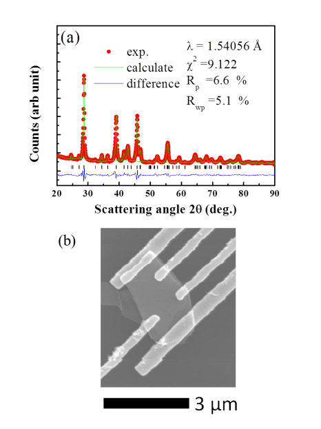
Figure 4.1. (a) GSAS refinement of powder X-ray data of a BSTS crystal. Red circles represent experimental results, the green line represents calculated results, the blue line indicates the difference, and the Bragg peaks of the BSTS are shown by the vertical lines, where Rp, Rwp, and ï£2 represent the goodness factors. (b) The SEM image of a BSTS 160-nm nanoflake.

4.3 Results and discussion
4.3.1 Thickness and temperature dependence of resistance
The considerable thickness dependence of electrical transport showed a transition from semiconducting to metallic behavior as the bulk content is reduced, as shown in Figure 4.2 (a). For the thick specimens, the thermal activation energies given by the Arrhenius law were 4.3 meV (140 μm), 3.5 meV (49 μm), and 2.37 meV (7 μm). The smaller activation energy of thinner specimens can be explained by the increasing contribution of surface states [12-13, 40-41]. In 140-μm BSTS, a significant deviation occurred below 20 K from the fitting to a three-dimensional variable-range hopping model (3D VRH) with Rxx is approximately exp[(T/T0)-1/4] [13], indicating the existence of a parallel metallic conduction of surface states [the inset in Figure 4.2 (a)]. According to Eq. 4.1, the total conductance G° of a specimen with a thickness t can be formulated as
G° = Gs + ï³bt, (4.1)
where Gs is the surface sheet conductance, and σb is the bulk conductivity [38,42]. Gs =36.2 (e2/h) and ï³b = 4.14 (e2/h) μm−1, which resulted from the fit of thickness dependence of conductance to Eq. 4.1. For a 200-nm nanoflake at 2 K, up to 90% of the contribution from the surface state was obtained, as shown in Figure 4.2 (b).
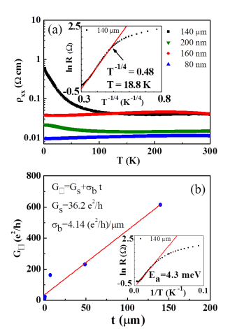
Figure 4.2. (a) Temperature dependence of resistivity for BSTS specimens with thicknesses of 140 μm, 200 nm, 160 nm, and 80 nm. The inset shows the fit of 3D variable-range hopping to the 140-lm specimens. (b) Thickness dependence of sheet conductance; the red line is the fit with G° = Gs + ï³bt. The inset shows the fitting of the Arrhenius law to the 140-μm specimen.
4.3.2 Hall measurements of BSTS
To understand the semiconductor-metallic transitions, we focus on the charge transport behavior (Figure 4.3) and temperature dependence Hall measurement results of 160 nm specimen (Figure 4.4). Because of that the thickness seems like to the critical in between semiconductor and metallic transition. In Figure 4.3 (a), we gives three regimes in the temperature profile, one can obtain the nanoflake specimen with 160 nm thick showing metallic behavior which contrasts to its bulk. In the regime I, the bulk conduction dominates, as the temperature decreases the resistance increased which shows a general narrow-gap semiconductor behavior this can be attributed to freezing of the impurity band carrier in the bulk [27]. The regime II reveals a typical metallic behavior signature, the resistance decreases as temperature reduced, this can be explained as reduce phonon scattering and nearly constant carrier density (shown in Figure 4.4 (a)) with a decreasing temperature. In regime III, when the temperature is lower than 10 K, a slightly increases in resistance due to the bulk carriers freeze out [28]. Hall mobility measurements provide more clearly picture to realize the thickness dependence charge transport as shown in Figure 4.4 (b). The reduction in the degree of disorder or impurity of specimens can be obtained in Figure 4.4 (b) that the mobility enhanced as thickness decreased and their different temperature dependence trends. In thinner specimens (160 and 80 nm) the mobility shows monotonically increasing as decreasing temperature, surface dominate transport should play a more important role in this manner.
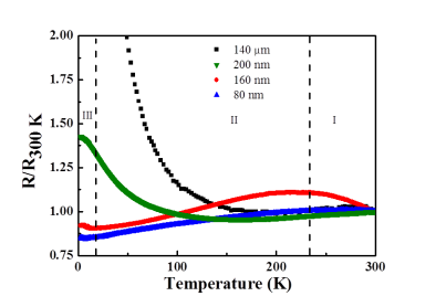
Figure 4.3. Temperature dependence of the normalized resistance of specimens.
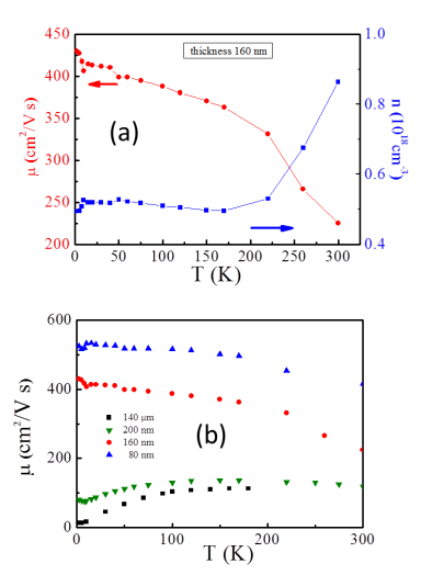
Figure 4.4 (a) Temperature dependence of the Hall measurement results of 160 nm thick specimen. (b) Thickness dependence of Hall mobility versus temperature curve.
4.3.3 Surface quantum oscillations (Shubnikov-de Haas oscillations)
Because successive empting of Landau levels (LLs) provides the nth minima in Rxx, the relation of the LL index n to the Fermi surface cross-section area AF can be described using the semiclassical Onsager equation: 2° (n + ï§) = AF ħ / eB.
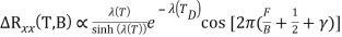
For the Schrodinger electron case, ï§ = 0, which results in a zero Berry phase. ï§ = 1/2 indicates the case of the Dirac fermion of TIs, which results in a ° Berry phase where the charge carrier is immune to localization. The temperature dependence of resistance for a 200-nm nanoflake shows Rxx as a function of 1/B after a smoothing background subtraction, as shown in Figure 4.5 (a). Two sets of oscillation periods are marked; one with a black dashed line ([((1/B) = 0.041 T-1]) and the other with a blue dashed line (0.022 T-1) for the surfaces of the nanoflake specimen. The multicomponent nature of SdH oscillations originates from the Fermi-level positions of the two surfaces. If SdH oscillations are as a result of the two-dimensional electron gas (2DEG) formed with band bending near the surface, the corresponded carrier density differs in an order of magnitude [35] compared to the Hall measurement result [n3D = 3.5 ï‚´ 1018cm-3], which is obtained from the fit to low field B (±1T) data (Figure 4.5 (b)).
Figure 4.5 (c) shows the LL fan diagram plotted in 1/B versus nth oscillation minima in Rxx. The linear fit of the two-set SdH spectrum yields the intercepts of ï§ = 0.48 ± 0.3 for Surface 1 and 0.49 ± 0.02 for Surface 2, where ï§ values are closer to the theoretical value of 0.5 for ideal Dirac fermions. It is assumed that Surface 2 is the top surface because environmental contamination provides effective n-type doping [17] to the sample, which strongly influences the top surface. The specimens were closely stacked on the substrate to prevent the bottom surface from air contamination and electron-beam irradiation. Thus, the second set of SdH oscillations appears in the lower inversed field, shown in Figure 4.5 (a), which was probably from the top surface. In Figure 4.5 (c), the slope of one set of SdH oscillations provides the cross-section area of the Fermi surface [AF = 4.15 × 10¹⁷ m-2], and the Fermi wave number was  = 0.0363
  and the 2D surface carrier density was
  = 1.05 × 1012 cm-2 for the top surface (Surface 2). The second set of SdH oscillations resulted in AF = 2.32 × 10¹⁷ m-2 and
  = 0.02718 , and
  0.58 × 1012 cm-2 for the bottom surface (Surface 1).
Figure 4.5 (d) shows the fit of temperature dependence of SdH amplitudes to the Lifshitz-Kosevich (LK) theory [11, 43].The cyclotron mass mc = 0.075 me is the same as that reported [13]. Once mc is known, we can calculate the Fermi velocity and the Fermi level position to be vF = 5.6 × 10⁵ m/s and EF = 134 meV above the Dirac point for the top surface and vF = 4.19 × 10⁵ m/s and EF = 75 meV for the bottom surface. The high Fermi level position of the top surface is consistent with the results of environmental doping mentioned previously.
Due to the multiple component nature, the Dingle temperature is difficult to extrapolate from the SdH amplitude; therefore, Eq. 4.2 is used to fit the resistance data to the LK theory
 , (4.2)
where F is the frequency of SdH oscillations extracted from the slopes of Figure 4.5 (c), the thermal factor is  , and the Dingle temperature is
  [11, 43].
The solid red line in Figure 4.5 (e) shows the optimal fitted results of ï§ = 0.5 and ï´ = 1.11 × 10⁻¹³ s for the top surface, and ï§ = 0.35 and ï´ = 1.56 × 10⁻¹³ s for the bottom surface. The fitted ï§ values are close to theoretical value of 0.5 for ideal Dirac fermions. According to the Dingle analysis, the scattering time is approximately two to three times larger than that of the bulk BSTS [13]. Mobility is a measure of scattering time; therefore, it is possible to calculate the surface mobility μs = 2602 cm2V-1s-1 and the mean free path  = 62 nm for the top surface, and μs = 3657 cm2V-1s-1 and = 65 nm for the bottom surface. The surface mobility enhancement is consistent with the longer mean free path of the nontrivial topological Dirac state.
The surface contribution to the total conductance (Gs/Gtot = 84.8%) was consistent with the results obtained from the thickness dependence of conductance. Take the sheet carrier density into account, n = ns + nb t [44]. The mobility of the bulk channel was 12 cm2/Vs, which is close to the total Hall mobility of the 140-μm thick BSTS specimen, 13 cm2/Vs. The low Hall mobility of bulk carriers causes less interference with the surface Dirac fermions; thus, the enhancement of the surface contribution and quantum oscillations was detected in the specimens used in this study.
Figure 4.5. (a) Temperature dependence of resistance. Rxx is function of 1/B. n = 4, 5, and 6 are the LLs of the bottom surface; n = 6, 7, 8, and 9 are the LLs of the top surface of the 200-nm nanoflake. (b) Hall resistance versus magnetic field. The red dashed line is extended from the low B (±1T) fit. The inset shows the Fermi level positions of the top and bottom surfaces, respectively. BV is the bulk valance band, and BC is the conduction band. (c) The LL fan diagram plotted in 1/B versus the nth oscillation minima in the Rxx. (d) The fit of temperature dependence of the SdH oscillation amplitude to the LK theory. (e) R versus 1/B. The black curve is the experimental data, and the red curve is the fit to LK theory.
4.3.4 Weak anti-localization effect
In addition to SdH oscillations, the helical surface state was further probed using the WAL effect on the 200-nm BSTS. The WAL effect in TIs originated from the ° Berry phase, in which the probability of backscattering was suppressed as a result of the destructive interference of time-reversed paths. The angle field dependence magnetoconductance analysis is shown in Figure 4.6 (a). The sharp cusps of the magnetoconductance in the lower field region are features of WAL. The 2D nature of Dirac fermions associated with the ° Berry phase, which is dependent only on the perpendicular component of the applying field, was obtained by subtracting the background from the 3D bulk WAL contribution, ΔGxx(θ,B) = Gxx(θ,B) – Gxx(90°,B) (5), as shown in Figure 4.6 (b). Figure 4.6 (b) shows that low-angle data merge into a single universal curve [15]. The Hikami-Larkin-Nagaoka (HLN) [15] model is used to calculate sheet conductance [27], as given in Eq. (3):
 , (4.3)
where Gxx is sheet conductance, is the phase coherent length, and
  is the digamma function.
The value for ï¡ (-0.96) and (121 nm) were obtained for the 200-nm nanoflake. For the WAL effect in TIs, the prefactor ï¡ was equal to -0.5 for a single surface state [40]. The complicacies of topological surface states resulted in an experimental value ï¡ between -0.4 to -1.5 [38, 40]. In this study, the value ï¡ = -0.96 indicated the existence of two surface states.
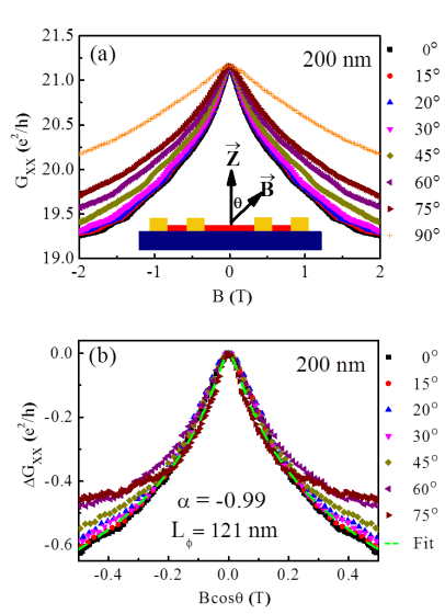
Figure 4.6. (a) The angle field dependence magnetoconductance of the 200-nm nanoflake. The inset is a schematic diagram of the measurement. (b) ΔGxx versus the perpendicular field component (B cos θ) for various angles. Low-angle data merge into a single curve (the green dashed line) fitted using the HLN model.
4.4 Conclusion
In this study, dominated surface transport was observed in BSTS nanoflakes. The thickness dependence electrical transport and the SdH oscillations illustrated that the surface states in the 200-nm BSTS nanoflake contribute to nearly 90 % of the conductance. The achievement of the surface-dominated transport is mainly attributed to the high surface mobility relative to the bulk channel. The observation of SdH oscillations provides clear evidence of surface Dirac fermions. Surface-dominated transport was further confirmed by the WAL effect showing 2D nature of helical Dirac surface states. Moreover, electrical transport transforms from semiconducting to metallic behavior, and mobility was enhanced when the thickness decreased, indicating that surface states plays a crucial role in the thin film limit. The high-insulating bulk state in BSTS nanoflakes provides opportunities for future quantum computation and spintronics applications.
Cite This Work
To export a reference to this article please select a referencing stye below:
Related Services
View all


DMCA / Removal Request
If you are the original writer of this essay and no longer wish to have your work published on UKEssays.com then please click the following link to email our support team:
Request essay removal